Ana içeriğe geç

Google Homeの分解

İngilizce
Japonca
Adım 6
Google Home Teardown: adım 0, 3 resimden 1. Google Home Teardown: adım 0, 3 resimden 2. Google Home Teardown: adım 0, 3 resimden 3.
  • Here's the source of our board removal strife: A layer of super sticky adhesive, keeping the capacitive board in contact with the plastic upper case.

  • This round green grid is half of an array of capacitors—with the other half buried in another, deeper PCB layer. By measuring the total capacitance of each row and column, the controller can detect when—and pinpoint where—your finger is modifying the capacity of the grid through capacitative coupling. Science!

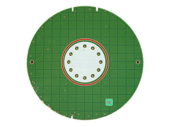
  • This side of the board also hosts an array of 12 status LEDs.

  • On the backside we find some chips:

  • Atmel ATSAMD21 32-bit ARM Cortex-M0+ microcontroller

  • Two NXP PCA9956BTW LED drivers

  • Two InvenSense INMP621 MEMS microphones—will only two be enough compared to the Echo's seven?

  • Ambient Light Sensor

さて、これが私たちが行ったボード取り外し作業の様子です。1枚の強力な接着剤シートがプラスチック製の上側ケースと容量ボードを留めています。

この丸くて緑色のグリッド上にキャパシタの配列の半分が装着されています。残りの半分はプリント基板レイヤーの奥深くに埋められています。各配列と縦列の静電容量を測ってみると、コントローラーが時間と正確な場所を探知することができるのです。言い換えると、自分の指が容量結合を通してグリッドの容量を変えているのです。サイエンスです!

基板のこちら側には12個のステータスLEDも配置されています。

裏側にはチップが埋め込まれています。

Atmel ATSAMD21 32-bit ARM Cortex-M0+ マイクロコントローラ

Two NXP PCA9956BTW LED ドライバー

2つのInvenSense INMP621 MEMS マイク—Echoは7つのマイクが付けられているのに対して、2つのマイクとは十分なのでしょうか?

環境光センサー

Katkılarınız, açık kaynak Creative Commons lisansı altında lisanslanmaktadır.