Giriş
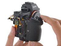
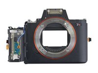
The a7R II is Sony's second shot at a professional-grade mirrorless interchangeable-lens camera, but this time, Sony claims it can keep up with any Canikon DSLR. While trial by fire may be the best way to judge a camera, trial by teardown is our specialty. With a $3,199 price tag and no reflex system, we hope this mostly-solid-state camera comes with an equally hefty repairability score.
Curious about what drives these new devices? Let us shed some light on them! Follow us on Facebook, Instagram, or Twitter to focus on the latest teardown news!
Neye ihtiyacın var
-
-
The a7R II has landed! Sony's much-ballyhooed second go at a pro-grade, mirrorless, interchangeable-lens camera has our full attention. Let's see what new tech makes this camera shine:
-
42.4 MP Exmor R CMOS back-illuminated sensor
-
BIONZ X image processor
-
5-axis in-body optical image stabilization
-
4K video recording
-
Fast hybrid AF system with 399 focus points
-
NFC and Wi-Fi connectivity
-
The specs alone are enough to give us itchy shutter fingers—but, first things first. It's teardown time.
-
-
-
The rear of the camera is adorned with an articulating 3 inch LCD. This is a TFT LCD display with 1,228,800 dots. Dots? What are dots? TIL a dot is (usually) a third of a pixel.
-
In short, less than an iPhone (326 for the iPhone 6), but certainly high-density. And that's good, considering that no mirror means no optical viewfinding.
-
The left side of the camera body houses plenty of I/O options—an HDMI micro connector, 3.5 mm stereo microphone and headphone terminals, and a micro-USB connector.
-
-
-
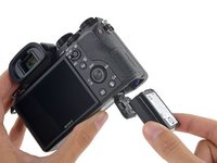
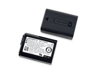
We find the same NP-FW50 7.2 V, 1020 mAh swappable battery pack as the original a7R and the rest of the Sony Alpha lineup—good news for anyone building a fleet of flagship mirrorless cams.
-
Sony kindly included not one but two batteries. You can also charge the battery inside the camera (USB adapter included), and even power the camera entirely via USB.
-
-
-
We turn our attention to the JIS screws securing the bottom plate, mouths watering in anticipation of the smörgåsbord of tech beneath...
-
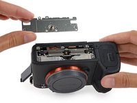
...And find the tripod mount plate.
-
It may not be glamorous, but the tripod mount slides out with ease, great news repairability. Tripod-happy owners can rest easy.
-
-
-
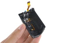
The bottom panel was a bit of a red herring so we investigate the LCD arm for weak spots.
-
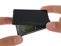
The rear LCD panel is connected by a thin ribbon cable that disappears into the back of the camera body. We'll probably have to deal with that before we can crack open this camera...
-
Luckily, a small door on the back of the display assembly opens the way to a tiny ZIF securing the cable.
-
We allow ourselves a brief detour to investigate the display before delving into the camera body.
-
-
-
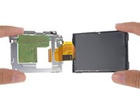
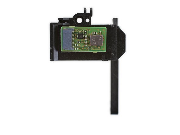
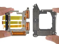
Peeling the LCD from the articulating bracket reveals a PCB packed with passives.
-
This little circuit board is probably a breakout board for the LCD, allowing for a thinner cable from the camera.
-
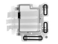
The capacitors probably reduce noise in the display; they're clearly visible as a little cluster of dark spots in this X-ray image, courtesy of our buds at Creative Electron.
-
Display technology is finally close to passing its Turing test: being indistinguishable from the mirror views in high-end cameras. This leap in tech has allowed for the viability of mirrorless cameras like the A7 series.
-
-
-
-
Once we extricate the LCD and its delicate flex cable, the parts start flying.
-
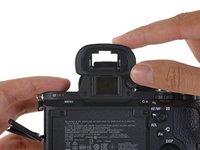
First up are the eyepiece and viewfinder frame. The eyepiece slides off for easy swaps; the viewfinder frame is held in place with a few screws.
-
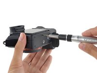
With some careful hunting, we find a few remaining screws hiding in the battery cavity. We're pretty stoked for a chance to use the telescoping driver handle in our Universal Bit Kit.
-
-
-
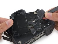
Now that the viewfinder frame and LCD panel have been removed, the rear housing pops right off.
-
All of the button's switches are mounted to internal components instead of the frame—so there aren't any delicate cables to worry about.
-
After disconnecting a single cable, we tease out that very mounting frame and the rear button assembly attached to it.
-
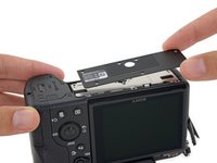
Next off is the multi-format card reader. It comes quietly.
-
We're secretly hoping this camera plays Nintendo DS games.
-
-
-
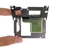
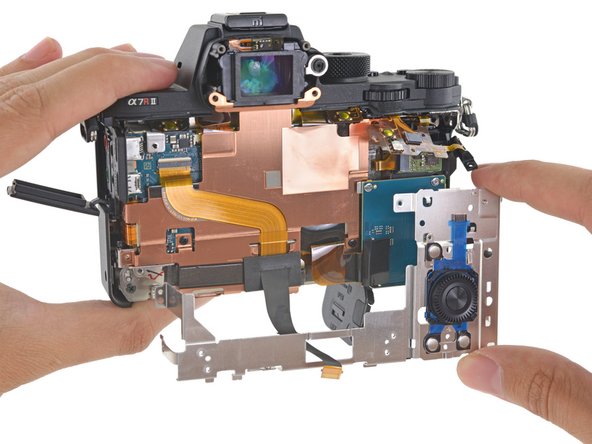
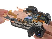
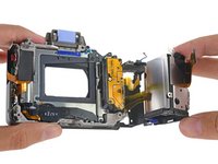
With the rear housing and button assembly removed, the motherboard shield comes out with very little resistance.
-
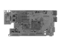
Getting our first clear view of the motherboard, we set to work disconnecting every ribbon cable created since the dawn of time.
-
-
-
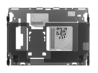
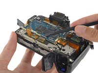
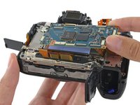
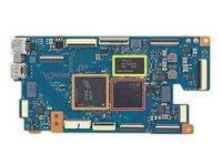
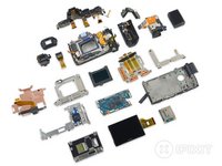
We hoist the motherboard out for inspection, finding:
-
Sony CXD90027GF SoC
-
Micron Technology 5FA98 JWB39 eMCP
-
SK Hynix H5TC4G63CFR 4 Gb DDR3L SDRAM
-
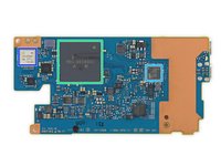
And on the reverse side:
-
Sony CXD4236-1GG, likely a newer version of the CXD4236GG image processor
-
Fujitsu MB9AF004 32-bit ARM Cortex-M3 processor
-
Murata KM5601002
-
-
-
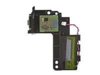
This is the part where we get a grip, a camera grip that is.
-
An access port allows us to remove the final screw securing the front grip to the body.
-
Camera brand-fans live and die by their adjustment wheels. The grip features the forward spinner and shutter button, as well as the Wi-Fi antenna.
-
-
-
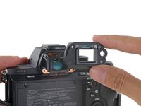
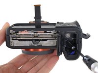
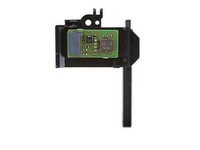
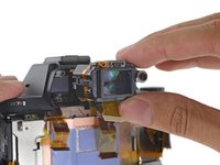
Back to the viewfinder—turns out we can pull it straight out of its cavity. With its frame previously dispatched, it was only held in place by a gummy thermal pad.
-
Why the thermal pad? Might have something to do with the 1.3 cm XGA OLED. With 1024 x 768 pixels in half an inch, that's 2,560 ppi. Wowza.
-
The lens assembly even works as a standalone upside-down-maker! Aren't optics cool? That logo sure is.
-
-
-
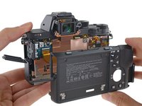
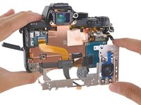
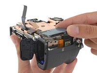
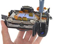
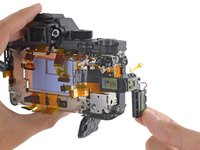
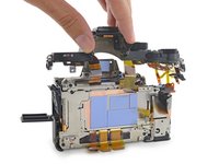
Hats off to you Sony! You've got our teardown engineer tired, but not beat. The upper case assembly pops off and steps aside for a glimpse at the goods.
-
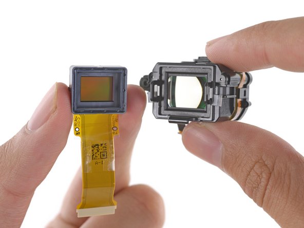
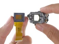
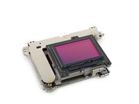
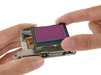
Eager to get our first look at the new Exmor R CMOS sensor, we extricate the entire sensor assembly from the camera. The rest of the body feels like an empty husk without the hulking sensor and stabilization cradle.
-
-
-
A quick detour before we proceed to the magnets: we pluck the a7R II's 42.4 MP image sensor from the stabilization system.
-
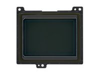
With the CMOS sensor in the wild, we get a clearer view of what's been touted as the world's first back-illuminated 35 mm full-frame sensor.
-
The square hole in the sensor's PCB also hints at a tricky assembly process—it's likely a cutout used to accommodate the vacuum nozzle that holds the sensor during assembly, as evidenced by the small patch of scratches at the center of the cutout. A peek with the X-ray reveals the array of solder balls that sandwiches the whole thing together when it's done.
-
-
-
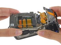
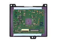
Is that a Force Touch trackpad? No, it's an exposed view of the a7R II's sensor-shift stabilization hardware. Sony's marketing team named this the 5-axis SteadyShot. Fancy.
-
The central tray of the stabilizer holds the image sensor, and is home to three electromagnets, each a component of a voice coil, an electromechanical device used for incredibly fine positioning.
-
These coils live in the magnetic fields of their permanent magnet buddies—which means slight variations in power to the three coils generates forces in a variety of directions. Enough variety to adjust the sensor on five distinct axes. Not a small feat for a full-frame camera.
-
-
-
A7R II Repairability Score: 4 out of 10 (10 is easiest to repair).
-
The battery can be easily replaced without tools.
-
The tripod mount and viewfinder can be replaced without disassembling the camera body.
-
While very difficult, the rear LCD panel can also be removed without disassembling the camera body.
-
Accessing anything inside the camera requires removing the complex rear LCD panel first.
-
Internal components are very intricately organized; repair without a service manual would be very difficult.
-
Lastly, a hearty shout-out to our friends at Creative Electron for their X-ray imaging wizardry. Thanks guys!
-


35 Yorum
Yeah, Wondering also about weather sealing.