Giriş
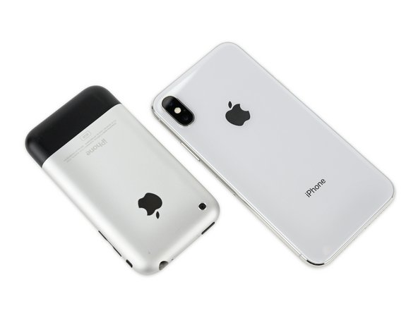
Ten years ago, Apple introduced the very first iPhone, and changed the world. Today, we're taking apart Apple's 18th iteration—the iPhone X. With its rounded edges and edge-to-edge display, we're sure this is the iPhone Steve imagined all of those years ago—but now that his dream is realized, will it be as influential as the first? Time will tell, but for now we'll be doing our part to help you decide. Join us as we open Apple's crown jewel to see what makes it shine.
A big thanks to Circuitwise for hosting our teardown down under, Creative Electron for X-ray imagery, and TechInsights for IC ID.
It's serendipitous that we're in Sydney, because we've got an Australia store now. As we learn more, we'll be posting on Facebook, Instagram and Twitter. We've got a newsletter too if you're the email type.
Neye ihtiyacın var
Videoya Genel Bakış
-
-
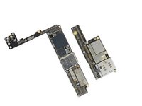
The iPhone X is here! Here's the fillin' inside that glass sandwich:
-
A11 "Bionic" chip with neural engine and embedded M11 motion coprocessor
-
5.8 inch "all-screen" OLED multitouch Super Retina HD display with 2436 × 1125-pixel resolution (458 ppi)
-
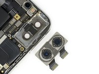
Dual 12 MP cameras (wide-angle and telephoto) with ƒ/1.8 and ƒ/2.4 apertures and OIS
-
7 MP TrueDepth camera with ƒ/2.2 aperture, 1080p HD video recording, and Face ID
-
Support for fast-charge and Qi wireless charging
-
Our A1865 global unit has broad cellular band support as well as 802.11a/b/g/n/ac Wi‑Fi w/MIMO + Bluetooth 5.0 + NFC.
-
-
-
The iPhone has come a long way in ten years—so long, in fact, that the design has cycled back a bit, and this iPhone looks more like the original than we've seen in a long time.
-
As was the case with the iPhone 8 earlier this year, Apple has banished the unsightly (and environmentally responsible) regulatory markings from the back of the iPhone X.
-
Jony finally has the featureless smooth backplane you know he's always wanted. Hopefully these phones still make it to recyclers without the hint and don't get dumped in the trash.
Here in Ireland (and I guess across the EU) we have the ‘Designed by Apple in California Assembled in China’ text, the CE mark and the ‘no dumping’ bin graphic still in place.
Anyone who thinks the markings on the back of the iPhone will influence whether it is recycled (rather than the trade-in value, accessibility of recycling facility or a customer’s own environmental awareness) has probably shoved a spudger too far up their nose.
Where did you get that minty fresh first-gen iPhone? Is it part of iFixit’s collection?
I’m really glad they took out the regulatory info on the back. It simply didn’t need to be there. You know you’re not supposed to throw an electronic away.
-
-
-
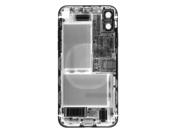
Before we dive in blindly, let's get some
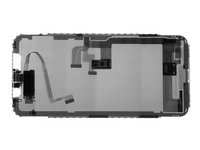
10-rayX-ray recon from our friends at Creative Electron. -
Here's what we found:
-
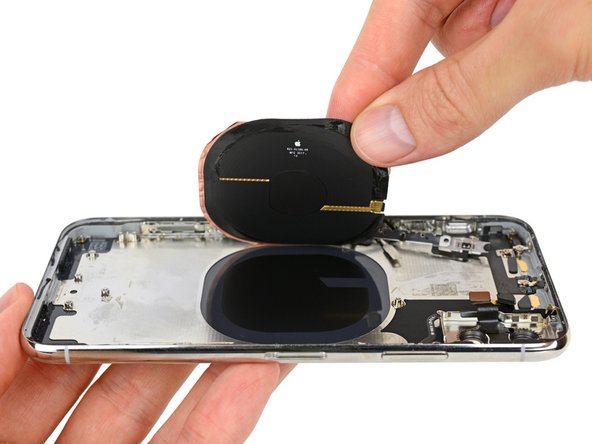
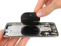
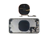
Not one, but two battery cells. That's a first in an iPhone!
-
A super-tiny logic board footprint. Based on the overlaid solder points, it looks like there are two stacked layers.
-
To make room for the extra front-facing sensors, the earpiece speaker has been shifted down quite a bit.
-
There's a mysterious chip between the Taptic Engine and lower speaker—we're curious to see what's down there!
-
-
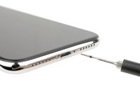
Bu adımda kullanılan alet:iOpener$17.99
-
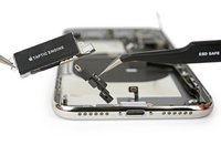
This pentalobe looks weirdly unfinished. The bottom screws are more like pins if we're honest.
-
This screw moves the threaded section from the display to the steel frame, and extends the unthreaded section into a freakishly long pin.
-
Our best guess is that this allows the display a bit of flexibility, while also allowing it to move its mounting bracket toward the interior of the phone, incidentally making room for a beefed-up Lightning connector.
-
Luckily, it looks like they haven't rearranged too much else, as our typical trifecta of iOpener, iSclack, and iFixit Opening Picks works as in the past.
-
That means no significant change in resistance, and the OLED is well supported by a frame, unlike some displays we know.
-
-
Bu adımda kullanılan alet:Mako Driver Kit - 64 Precision Bits$39.95
-
Looks like sideways-opening iPhones are here to stay. Apple surprised us with this little trick on the 7 Plus, but by now it's standard.
-
This single bracket covers every logic board connector—we've never seen this kind of connector density.
-
And once again, we're faced with tri-point screws standing sentry over any repairs once you get past the pentalobe screws guarding the door.
As mentioned above.
sean -
fixed i guess
My bracket only has 4 screws - the second from top (towards the right side of the phone) is missing - I bought the phone direct from Apple on launch day. Pretty surprised! Anyone else ever had missing parts?
-
-
-
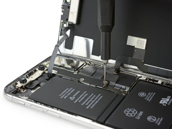
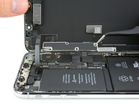
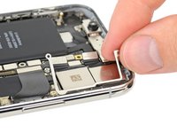
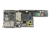
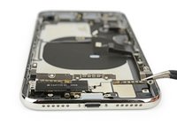
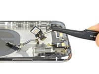
After freeing the massive unibracket from the logic board, we can finally steal a peek at the hardware powering Cupertino's latest flagship.
-
We'll get a better look at the hardware on the display later, for now we satisfy ourselves with an X-ray—turns out that mystery chip is mounted to the display!
-
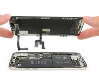
For a change of pace, the display lifts off and leaves the front-facing camera behind.
-
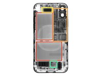
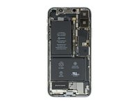
This body shot confirms the layout we observed in our X-Ray recon: most real estate is occupied by the new dual-cell battery, and the logic board has shrunk significantly.
-
-
-
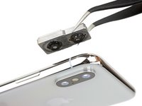
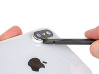
The dual rear camera has a beefy bracket that looks like it might offer some bendgate-proofing support for the delicate components.
-
The cameras are additionally secured to the rear case with some foam adhesive to keep things from jostling out of place. These cameras really need to stay put for Portrait Mode and similar features to work their magic.
-
Surrounding the camera housing cover glass, you can see tiny spot welds likely holding the walls of the camera bump to the case.
Might that beefy bracket be made of Liquidmetal (see https://en.wikipedia.org/wiki/Liquidmeta...)? That is, is it surpisingly stiff? Apple has an exclusive license to use Liquidmetal in consumer electronics, but seems not to have used it extensively.
-
-
-
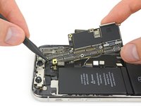
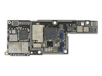
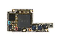
We finally free this most-dense of logic boards to get a closer look.
-
This miniaturized logic board is incredibly space efficient. The density of connectors and components is unprecedented. Ounce for ounce, even an Apple Watch has more bare board.
-
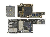
The compact iPhone X board manages to pack more tech and still make the iPhone 8 Plus board to its left look gangly and expansive.
-
Comparing the footprint of the two boards, the iPhone X motherboard is about 70% of the size of the iPhone 8 Plus board—that's a lot more floor space for battery.
If that happens, how will users switch to other networks and install SIMs in their phone when they go abroad to avoid outrageous roaming charges?
-
-
-
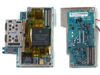
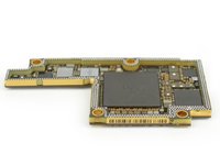
How did Apple put even more tech in 70% of the footprint? By folding the board in half, of course.
-
The two halves are soldered together, so we got some help from our hosts Circuitwise and their BGA hot air rework station to separate the layers.
-
With the pieces separated, we tallied the area of all of the separate layers, and added it up to 135% of the iPhone 8 Plus logic board's area. Way to go putting more into less, Apple.
-
The iPhone X logic board is the first double-stacked board we've seen in an iPhone since the very first iPhone (third photo).
You are missing the point. These are connecting the board physically, but there is no communication through those vias. You can see the other side of the board has all the connectors to flex. (On both boards). The third board act as a super stiffener to prevent overheating causing bending on the board. Great design!!!
Sorry Ramiro the outer row are shielding (ground) the 2rd & 3rd rows are comm lines between the boards (interposer board).
Dan -
Does the folded design take up more vertical space than the old logic board design, and if so, how did Apple account for this increased vertical space?
Was there vertical space open to begin with or does something in the design allow for more vertical space (i.e. the OLED panel is thinner)?
Thanks!
Yes, I think the OLED panel is considerably thinner. The X and 8 are pretty much the same thickness, so I think that that yes, it’s solely because of the OLED!
So Richard your assertion is that the silvered bumps all around the two boards are the vias? With a pitch of, what, 300µ?
The MacRumors article yesterday referred to an interposer between the two main boards, but I don’t see any such. Was MacRumors wrong, or am I missing something?
The outer perimeter of “silver bumps” aka solder balls is most likely all connected to ground. The rest must be signals. There is not enough cabling to support the required amount of signals between the two boards.
The interposer is still attached to the half in the top of the picture. The border of solder balls is higher than the rest of the PCB. This is required due to the night of the components on each PCB.
Truly incredible design. Passes data without cabling, affixes the two boards to each other without hardware, and creates an EMI shield without extra metal
Is that a piece of flat flex connected across two parts of the lower board? going right under the middle screw hole
It’s the ribbon from the camera’s which is poking up.
Dan -
Dan, I don't think so. Its completely sealed inside the sandwich
Thats just a kapton insulator sheet inside the sandwich. I thought you were talking about the other image.
Dan -
I believe it time to find some more of my good old LCD bonding 9703 3M anisotropic tape. That might be the ticket for servicing that motherboard. Still have some tape in stock, so my shop will service that motherboard, when parts become available.
Have a good weekend all.
Jan
How did apple manage to take out heat from their processor? I still couldn’t understand how is this working…
You are all wrong :-) look at the RF board, there isn’t a signle trace routed from the armada of solder-pads, so I’d say they’re purely mechanical & GND /tekhead
You do understand the PCB is made up of layers.
Their won’t necessary be any visible traces on the surface besides what space is there! It’s so packed the lines would need to be buried inside the layers. One of the functions of via’s is to bring signals up and down the layers, clearly Apple is leveraging this here through the interposer board.
Dan -
@kyle - Found a good image set from Tech Insights! Here’s the side views http://www.techinsights.com/uploadedImag... and http://www.techinsights.com/uploadedImag...
There’s a lot of need for intercommunication between the RF and the main CPU. There’s no other interconnect between the two boards. The perimeter vias have to be a communication bus.
-
-
-
-
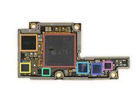
On the first half:
-
Apple APL1W72 A11 Bionic SoC layered over SK hynix H9HKNNNDBMAUUR 3 GB LPDDR4X RAM
-
Apple 338S00341-B1 power management IC
-
Texas Instruments SN2501 battery charger
-
NXP Semiconductor CBTL1612A1—Likely an iteration of the 1610 tristar IC
-
Apple 338S00248 audio codec
-
STMicroelectronics STB600B0 power management
-
Apple 338S00306 power management IC
What are those “white stickers” in different shapes on the board? Are they the typical for checking water damage? Are the same shapes stickers related to each other in any way? Function?
Some of these components have a polarity. The white or black dot or a triangle denotes positive or anode end of the cap or diode.
Dan -
I think those are inductors, and the white spot indicates the right direction for them to go on the board.
Which is A11 Apple processor module part number, on same package row as SoC die designation APL1W72? The A11 Apple processor module part number has a format 339S004xx. The A11 photos are without sufficient contrast and difficult to read.
No help on A11 Apple processor module part number in this analysed iPhone?
Dimitar -
Is it me or are all the surface mount capacitors misaligned on the far right end? One is barely making contact with the pad. It’s like someone fudged it with their thumb picking it up.
I think that happens when you desolder it with hot air. It heats up the whole board.
which one of these chips are the thermal monitor? I have a damaged IPhone X that says the thermal monitor is dead.
I would be surprised if there is a separate chip for thermal monitoring. It’s more likely a function buried in one of the other ICs, probably one of the power management devices.
-
-
-
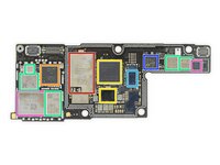
Apple/Murata USI 170821 339S00397 WiFi/Bluetooth module
-
Qualcomm WTR5975 gigabit LTE transceiver.
-
Qualcomm MDM9655 Snapdragon X16 LTE modem and PMD9655 PMIC. But Apple is dual-sourcing the modem, and TechInsights found an Intel XMM7480 (PMB9948) in their A1901 model. Even though the modem is capable of it, Apple isn’t supporting Gigabit speeds with the Qualcomm part.
-
Skyworks SKY78140-22 power amplifier, SKY77366-17 power amplifier, S770 6662, 3760 5418 1736
-
Broadcom BCM59355 wireless charging controller
-
NXP 80V18 PN80V NFC controller module
-
Broadcom AFEM-8072, MMMB power amplifier module
Vic Lau, Qualcomm makes good chips at good prices, so there isn’t any reason Apple shouldn’t use them.
Yes, there is. They're suing each other.
If apple moves away from Qualcomm we can definitely expect a higher price tag on the next iteration of the iPhone
DAXimus -
The suing didn’t stop Qualcomm to get enough order apparently.
On the contrary,a higher price for customers to purchase iPhoneX seems to be the only result.
Theres more to it than the chips, It appears there are some licensing payments owed. Here’s a bit more Apple may completely drop Qualcomm as a modem supplier on future iPhone models
Dan -
Both those chips are present in Iphone 8 plus as well. They are just in different locations. Check step 10 in Iphone 8 plus tear-down.
Actually both the chips are required. MDM9655 is a baseband modem, and WTR5975 is a RF transceiver.
my Logic board has some damages to the circuit. I was thinking about buying another logic board (say iCloud locked) and transfer all if these chips. Will it work? Has anyone done it?
-
-
-
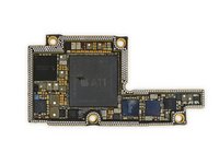
And on the outside of the logic board sandwich:
-
Toshiba TSB3234X68354TWNA1 64 GB flash memory
-
Apple/Cirrus Logic 338S00296 audio amplifier
-
Bosch Sensortec BMP282 pressure sensor
-
Bosch Sensortec gyroscope/accelerometer
Kapton tape on the underside for insulation, yeah
looks like the backside of the reader
anyone can tell that the storage its a TLC or MLC?
And what to say about those two capacitors a bit off their solder points, almost touching the capacitor next to it ? Should’ve been failed in quality control, or visual inspection at least, no ?
Or …. Could it be the heat from you guys separating the boards, that made the components wiggle a bit and shift from their correct placement ?
The second one. ;) We’re doing this for the first time, often under less than ideal conditions, in a pretty big hurry. People who are more skilled and patient than I am can separate the boards and solder them back together flawlessly.
-
-
-
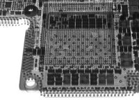
Okay, so Apple made a PCB sandwich, but how does it work?
-
Here, the A11 SoC lies nestled at the center of the main board. You can get a sense of the 3D structure of the board from the X-ray photos. The cylinders around the edge are holes filled with solder connecting the two boards.
Dan, most through-hole vias are hollow.
-> iFixit,
look again, there are no traces routed from those, so I don’t think any data is travelling through those. It’s just ground.
any relevant high-speed bus wouldn’t work well routed in that manner.
main board is the “computer“ where all the flexes come in to connect to screen & peripherals.
the rf-board is purely networking so very few wires has to connect between the main ARM and that board.
Albert, Review the comments in Step9 there is no other means for the two half to communicate with each other other than the vias and yes some are shielding (ground)
Dan -
Lel. Yeah. Those are just via stiching for shielding.
Maybe vias are security related. PCI homologation request for tamper-proof protection against encryption keys reading strait from RAM.
I think you are right! but I’m not sure that which chip to process security function.
-
-
-
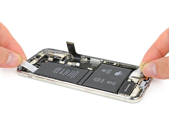
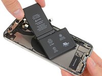
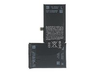
The new dual-celled battery has four pull-tabs, similar to the shorter ones we found in the 8 series, albeit in an entirely new orientation.
-
This phone is packing a 10.35 Wh (2716 mAh at 3.81 V) battery, just beating out the 10.28 Wh 8 Plus battery—but still trailing the Galaxy Note8 with its 12.71 Wh behemoth.
-
The dual-cell design is more of a space-utilization measure than a capacity-changing one. Two cells allows for more creative shapes and placement, to best take advantage of the space left over by shrinking the logic board.
It might be my age showing but what type of Li-Ion supports charging up to 4.35 ? (I mean .. there’s the type that goes up in flames but .. ?)
It is just a more stable battery that can handle higher voltage without damage. Even my Cubot Note S has 4,35V max voltage battery (4.150 mAh).
Okay so I use this phone for all the photos of appliances that we take at Jackson Appliance Repair Company. The question I have is— is the battery itself waterproof? Or is the phone waterproof (protecting components inside) when it’s fully assembled?
The device is waterproof. Batteries really can’t be made waterproof as they have exposed contacts which when shorted would be dangerous depending on how conductive the liquid was (i.e. salt water).
Dan -
-
-
-
Hey remember that Face ID feature? In an unusual turn of events, we actually tested it before we tore the phone down. Turns out our IR-enabled video camera isn't fast enough to snag the dot pattern, but we can see the illumination alright!
-
History time: way back in the day, Microsoft made a nifty spatial sensor called the Kinect. The infrared dot matrix tech powering it was created by Israeli tech company PrimeSense.
-
Apple bought PrimeSense for a cool $360 million way back in 2013, and has surely invested hundreds of millions more since then bringing this to market.
-
Meanwhile, Microsoft was left in the lurch and had to scramble to develop a new sensing system for the Kinect 2. Perhaps now that the iPhone has a depth sensor, people will attach it to drones, too!
@kyle tell your design team to add a play button over the image, people can easily miss that it’s a video. I thought it was just an image, but saw the comment about he enjoyed watching the video - so i hovered my mouse and then that’s I figured it’s really a video. :)
It’s IR. Human eyes can’t see it, so unlocking with Face ID is essentially just staring at it, and from the user’s perspective, it magically unlocks. No visible flashing here!
Jody, the flashes are invisible to the human eye. In the video you can hear the guy with the phone asking if the cameraman can see the flashes, because you need a special camera to view them. It’d be like staring into the end of a TV remote control and pushing buttons.
Not for me. I can see infrared easily.
Esa luz que nosotros no vemos, sera dañina de tanto uso ?. Porque desbloqueamos el telefono muchisimas veces al dia.
That light that we do not see, will be harmful of so much use? Because we unlock the phone many times a day.
Here’s a good vid on the FaceID projector lighting up someones face: https://youtu.be/OvVKnC6gGtg Jump to 5:50 to see it.
so why MS did not buy ++PrimeSense?++
Having designed a lens system for Occipital’s Structure sensor (which is also a Prime Sense derivative). The structured light emitter, which is actually a laser; vibrates to create the pattern that bathes your face. I am pretty sure the structure light source does not have the power to do anything besides scan your face, but also the infrared camera is lens system is probably tuned for 300 mm-500 mm unlike the Kinect(1), ASUS XTION or PrimeSense’s own early versions, which have a much longer range. If anyone is interested in doing more than just face scanning, check out Occipital’s website.: https://structure.io/ .
i wonder who makes the sensor subassembly - that must be a very intricate design; tying the processing and interface to the VCSELs that generate the light powering the activity
-
-
-
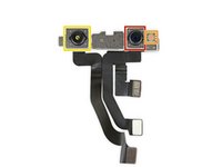
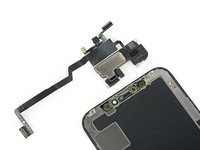
We turn our attention to the top of the phone to find the much anticipated
mini KinectTrueDepth camera system! This system rallies a team of sensors to bring facial recognition to the X. -
Step one in this system: the flood illuminator embedded in the display blasts your face with infrared (IR) light.
-
Next, the front-facing camera, marked in red, confirms the presence of a face.
-
Then the IR dot projector, far right, projects a grid of dots over your face to create a three-dimensional map.
-
Finally, the IR camera on the left reads this map, and sends the data to the phone.
-
Under the hood, the X works some seriously fast software magic to bring all these pieces together and figure out if you're you, or your evil twin.
Surely the ir camera senses the ir flood projector, not the standard camera…
There are three IR light sources used: The small pencil beam to see if the phone is face down or next to ones face (proximity) which uses the camera as the sensor (located just to the left of the speaker slot from the front). Then there is the flood illuminator which lets the camera ‘see’ if you are there (to discriminate there is a face present) just to the right of the camera. The third is the dot projector (on the right side of the speaker slot) to ID you. The same camera is used for all three functions no special IR camera here.
Can I buy that TrueDepth system?
Has anybody figured out, if this part is replaceable? I hope this isn’t handled like the TouchID which is locked to the logic board?
-
-
-
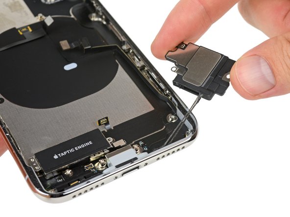
The end is in sight, and we're powering through the remaining components in the rear case.
-
This first little bracket is covered in spring connectors and EMI grounding fingers, and has a ribbon cable stuck to the back.
-
Next out is the lower speaker enclosure, replete with ooey gooey waterproofing adhesive around the port.
-
And lastly, the Taptic Engine and famed barometric vent are freed. Apple's Taptic Engine continues to be a linear oscillator vibration motor.
Are there two speakers at the bottom?
Nope just the one lower speaker. The second speaker is mounted to the upper portion of the display assembly.
How is vibration motor installe, it is glued or screwed?
A: Screwed. ;)
Do you sell replacements of the little bracket that is covered in spring connectors and EMI grounding fingers, and has a ribbon cable stuck to the back? As I was removing my screen to prepare for a replacement I saw that it had some damage. I don’t want to purchase a replace screen and find that it won’t work because of the damage to this part.
Caleb for some strange reason iFixit do not sell the EMI Grounding Finger plate nor do they sell the wifi flex cable that is attached to the underside of that plate. I had to go to Amazon to source a replacement for both. I think they should also stress how delicate those grounding fingers are, they are like tissue paper and can be damaged very easily if touched so take extreme caution when removing and reinstalling the plate and the attached flex cable.
Do you have links?? I can not find it.
Nice and informative post very helpful thanks for it, MS OFFICE 2019 MAC with lifetime license 70% Off.
Does anyone know the purpose of this bracket "covered in spring connectors and EMI grounding fingers"? What would be the possible side effects if it was damaged?
-
-
-
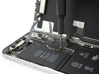
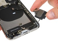
In fine form as always, our teardown engineer demonstrates dual tweezer technique to remove the Lightning connector.
-
Good news for anyone with the wiggly charging cable blues: the Lightning connector is looking extra-reinforced, with a wider bracket that screws into the sidewall of the frame.
-
It also features through holes for the exterior pentalobe screws to pass through and key into the display, as we saw earlier.
I don’t think it really matters. Apple’s Lightning Connector is double sided, so EVEN IF they DO have contact points on both sides, they probably would have wired them together anyway.
The Lightning connector IS double sided, however the pins are NOT NECESSARILY physically tied together in the connector; ergo it actually supports 16-pins, not 8. So it DOES matter. A double-sided port could hypothetically support Thunderbolt, or 2 USB3 channels. And we have seen, inexplicably, a double-sided port from Apple before in the iPad Pro. A fully 2-sided Lightning connector/port could be functionally as capable as USB Type-C, minus the legacy USB 2.0 lanes. (The Type-C connector ALWAYS maintains a legacy USB 2.0 pair; Apple would have no need for that legacy combination if Thunderbolt was their forward-looking target.)
Scott,
Apple has already defined the connector https://en.wikipedia.org/wiki/Lightning_... I doubt they are going to mess it up making it polarized directionally at this point.
Dan -
There are 2 separate parts here. One is the Lightning connector and the flex cable under it is the loud speaker flex cable.
-
-
-
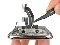
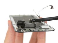
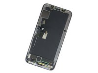
With the main assembly picked to bits, we turn our attention back to the display. The first thing to pop out at us is the earpiece speaker, newly redesigned with a cool duct to channel sound out of the display.
-
Carefully extricating the upper display components yields the most complex upper display component collection we've seen yet. It's home to a loudspeaker, microphone, ambient light sensor, flood illuminator, and proximity sensor.
-
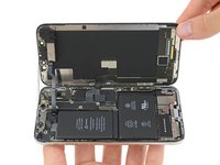
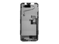
After picking off all the modular bits, we're left with a bare display.
So what was that mystery chip first shown in the x-ray pictures?
Where can I find a replacement upper display? Accidentally tore my wire ribbon slightly…
-
-
-
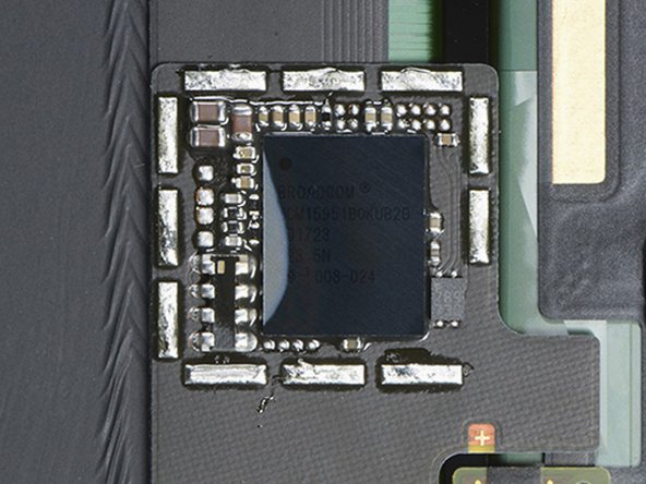
Time to get a look at that mystery chip! With a little help from our friends at TechInsights, we get a peek under the shields on the back of the display and find:
-
A Broadcom touch screen controller, labeled BCM15951B0KUB2G.
-
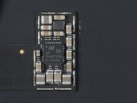
Also along for the ride: a new STMicro device we have not seen before, an OLED PMIC labeled 10 THADT733 X-139U.
The ST is more likely a boost converter, look at the inductors around it.
Too few pins to be a oled display-driver
-
-
-
Getting down to the X's bare metal, we run into another familiar piece to this densely-packed puzzle: the wireless charging coil.
-
Oh, and everything attached to it, including the volume buttons, ring/silent switch, and an unidentified sensor bracket.
-
We also peel out the other crazy multi-function cable from the top of the phone. This assembly's home to the quad-LED True Tone flash and the power button, much like iPhones of yore.
Is the Qi coil that needs to be unobstructed for wireless charging just the center circle the ribbons are attached to or is it the whole unit?
You can see the coil in step 3 x-ray images.
Just the big black coil.
Is there anything special with the charging coil? Do you think they are being modest and when airpower comes out it will blow away qi coils?
-
-
Bu adımda kullanılan alet:Jimmy$7.95
-
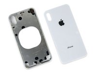
Bonus round: What happens when you break the rear glass on your brand new iPhone X?
-
After lots and lots of heat, we sheathed the spudger and drew our Jimmy. Like the iPhone 8 and 8 Plus, The X features a seriously glued rear panel.
-
After all of our careful Jimmying, we're still stuck: Unlike the iPhone 8's single piece rear panel, the camera bump overlaps the rear glass, and is meticulously welded to the metal frame beneath.
-
In this classic hand-stuck-in-cookie-jar situation, we can either cut off our hand (the camera bump) or shatter the cookie jar (the rear glass). Great.
Could you show the other side of the stainless shell? Is the glass apple logo and lettering at the bottom printed on the backside and glass layer over top?
Yup, same as the 8, you can see the bare inside of the glass here.
looking for this solution
How was the camera bump removed?
Destructively. It’s welded into place from the inside.
I find using a small flat head at each one of the weld points and rocking it left and right with a little force helps break the weld with less trouble than trying something large like a jimmy tool.
I opened the phone, removed the rear cameras, flash, logic board and battery, then wedged something underneath the rear camera bracket (which is spot welded to the camera bump) to break the spot welds to the camera bump. You’ll end up destroying the bracket (my replacement glass came with a new bracket and camera bump/lens) the bump will literally fall out once done. The rear glass can then be removed and replaced, then fit new camera bracket (and camera bump if damaged when removed).
Feel like doing a walk-through on this with photos for those less-inclined to break their new iPhone just because of a smashed back panel? :D
Absolute joke. After having spent all day painstakingly removing every single glass shard from the rear I find out that the bloody rear replacement glass doesn’t fit over the camera bump anyway…
Is there not a version that just fits over the bump even if it leaves a tiny gap ??? There is no way people will want their cameras/mics butchered. Failing that, it seems a bit excessive to strip down the entire phone just to remove a welded bracket. Frankly it is RIDICULOUS and I have been doing smartphone/tablet repairs from day 1.
It’s my own fault for not researching the subject. I wrongly assumed it was like previous models where it’s just held in place with adhesive tape.
This same kind of thing happened to me when the iPad airs came out and I thought it was still possible to do ‘glass only’. I think the only way I will learn is from not doing Apple repairs anymore!
Anyway well done Apple for catching me out yet again…..
Further update… Managed to find a seller on eBay who sells the rear glass covers with a slightly larger camera hole so it fits straight over the bump/lens. While this isn’t a perfect solution as there will be a bit of a gap it does makes it a million times easier and actually becomes feasible to do this repair (if you don’t mind hacking away at glass all day!).
My initial outburst was mainly because I was doing this job as a gesture of good will for someone and just assumed it to be straight forward. If it was my own phone or that of a close family/friend I would have just stripped it all down and done a proper job.
Hope this helps someone!
I use glass from aliexpress with normal hole with separate camera holder. If you put big hole glass you have the water resist problem.
Zeljko -
-
-
-
We hope you enjoyed your 22-course teardown meal. We found it very nutritious.
-
In case you missed the iPhone 8 or iPhone 8 Plus teardowns, you can check those out for some comparisons. And feel free to check out our Smartphone Repairability list for past device scores as well.
-
Thanks once again to our handy helpers, Circuitwise, Creative Electron, and TechInsights!
Is there any way to replace the mesh earpiece for this device?
-
- Display and battery repairs remain a priority in the iPhone's design.
- A cracked display can be replaced without removing the biometric Face ID hardware.
- Liberal use of screws is preferable to glue—but you'll have to bring your Apple-specific drivers (Pentalobe and tri-point) in addition to a standard Phillips.
- Waterproofing measures complicate some repairs, but make difficult water damage repairs less likely.
- Fussy cables tie unrelated components together into complex assemblies—expensive and troublesome to replace.
- Glass on front and back doubles the likelihood of drop damage—and if the back glass breaks, you'll be removing every component and replacing the entire chassis.


Son Düşünceler
Onarılabilirlik Puanı


(10 en kolay onarılabileni)
146 Yorum
Incredible and dense tech inside this iPhone - thanks ifixit!
Wow! So exciting!
Hello,
Could you give us more info about NFC antenna localization? I suppose it’s on top of the back panel (to avoid conflict with Qi )
Thanks
It’s the top bezel itself, as always.
Tom Chai -
From Iphone 6 to XS Max, its always been on top?
Exactly! Given the amount of effort they put into shrinking (or folding) certain parts, it’s great to see they’ve put in the same effort to not make it harder to repair. That any modern smartphone will never receive a 10/10 score due to the design choices is acceptable, so I’m happy to see there’s still a reasonable way in. Not like some tablet/laptop hybrids that are horrendous to even open up; yes I’m looking at you Microsoft!
is the face id hardware programmed to the phone like the touch ID was? that would make replacing it impossible by 3rd parties.
i know its not connected to the screen, but still it may be a common repair like it is now.
There isn’t really a reason why replacing the True Depth sensors should be a “common replacement” like the home button was. The home button had to be replaced because it was a physical piece of hardware that was pressed millions of times before failing. The True Depth sensor should fail rarely since it is protected under glass and won’t be hammered on constantly.
Very good! Finally different in the interior, the previous models were all the same!
Question which iPhone X version is this? with 2 Qualcom chips it looks like it is the Model A1865
We analyzed the A1865. TechInsights opened up an A1901.
Apple claims that in order to make the screen curve with the edges, they had to fold part of the OLED screen over to hide the display driver right under the screen. Would you be able to verify that?
yes, there was an animation in the promo video. Looked weird. I’d like to know how they get the cutout in there.
And how do the cutout pixels account to the display resolution?
Andi -
Yes I saw this too, can you investigate more into the OLED display? In the video at 0:30, Jony Ive says “the custom OLED panel was engineered to fold and seamlessly combine with the external surfaces.” Their computer rendering really makes it appear there are hundreds of hidden pixels being illuminated. https://youtu.be/K4wEI5zhHB0?t=30s
Sweet! I’m actually impressed by the efficiency of this.
The picture of the sandwich board is tilted and out of focus. Please retake from directly above
Hey Mitch! We have top down photos of the logic board in steps 9, 10, 11, and 12! Check them out! The photo in step 13 is meant to describe depth, so the angle the focus on the chips inside is intentional!
Please post XRay Wallpaper of the iPhone X! You guys are the only ones that do it right!
Just snag the xray ‘wallpaper’ off the enlarged picture above… o.O
From a boardlevel repair perspective I sense this is mostly game over.
Separation of the two layers requires an amount of heat applied to the whole structure pretty much all soldering folks would consider unsafe including myself.
Lets all hope very strong that this design improves mechanical stability to a point where we wont have breaking solder joints any more and improved circuitry preventing most common damages. The level and style of catch up game with the repair industry apple plays here is disconcerting.
After settling with recent macs not to be considered buyable because of &&^&^$^ all components being soldered in and tethered added to ridiculous toylike features driving stupid prices now the iPhone is also beyond what I am willing to accept for such money.
Its depressing to see how fast apple from year to year is becoming more about profit and money and less about tech and users.
I wonder how long I have to wait until some other player comes up with a real alternative in terms of user experience.
Yes i agree, what they did will make repairs harder you can see in this pictures some components moved from their place after separation which is a bad outcome.
Have you considered the Essential Phone? It seems like they may have something special over there…
Gino J -
I have to agree. I started out in 1980 with my bsee degree repairing Apple 1’s 2’s and 3’s with an oscilloscope, soldering iron and the latest copy of the ic circuit handbook. I have not been thrilled about Apples progression from everyman’s or women’s mac to unserviceable sometimes throw away stuff that needs cottage industries to support what they can, when before it was mainstream repair with dig this, a service door!.
@Ross Elkins: The Apple 1, ][ and /// were designs based on 7400-series TTL logic. Do you have any idea how big, power-hungry (and expensive!) devices like the iPhone would be, if they were designed with 7400 chips? If it would even be possible (which I seriously doubt), the PCBs stuffed-full of TTL logic would easily cover a football field, would require a 1000A power supply, and would cost $100,000 (or more)!!!
For you to even mention the repairability of stone knives and bearskins designs (no offense meant to Mssrs. Wozniak and company) like the first few Apple computers in the same breath as state of the art, massively-integrated product designs like the iPhone X strongly suggests that you wasted your money on that EE degree; because you certainly haven’t been keeping up with technology, even at a lay,an’s level.
Yes, serviceability has definitely lost ground to compact design over the years. There are trade offs everywhere and either we carry around a brick with a removable back panel for component repair/replacement access, or have the smartphone design we do today where it's practically an extension of our body. I'm for the latter.
I do love iFixit teardowns though, daring to go where no one is intended to.
I salute you, iFixit!
gamma
@atomicsymphonic Umm… you have to FREEZE it to get it open! Essential Phone Teardown It got a repairability score of 1.
Does the bottom left of the phone still just have a dummy panel covering the speaker grill?
If you’re thinking of the barometric vent, then yes! You can see it in the third image on step 17.
It looks like the mysterious chip was attached to the lower speaker…any idea what it is used for?
It is still mysterious!
Does the mystery chip possibly contain the data for the user’s facial recognition? Apple said that data would be stored on the phone only - and nowhere else - out of privacy concerns.
HL Dash -
Were you able to verify that face recognition still worked once the phone was re-assembled?
Facial Recognition works. But proximity sensor has to be swapped over to maintain Face ID after a screen swap.
iv tried today to swap screens on two iPhone X without swapping over any parts, just the screens and Face ID stopped working on both. ill try later to swap the proximity sensor to see if that fixes the Face ID.
roy -
I swapped two screens from one to the other on the iPhone X and Face ID stopped working on both. ill try later to see if swapping the proximity sensor fixes the Face ID not working.
roy -
Should be much easier to repair without the virtual touch id button.
this looks like a science fiction movie, very big WOW
Be nice if the person breaking down the phone, or at least the one who writes up the Teardown, had some engineering training, some of the text above was completely unintelligible, unscientific and used wrong terminology in descriptions. Apart from that, though, great! LOL
And you’re perfect in everything that you do right? If you’re so smart you should have filtered through all type O’s and kept your rude post to yourself, JACKASS!!
Stay tuned ;)
The next thing to go is the nano sim tray for sure it's so large compared to the logic board.
Apple’s almost definitely going to replace it with an eSIM in the next model. I sure hope so. https://www.blog.google/products/project...
What about the screen essentially folding backwards on top of itself? I was wondering about that in a tear down like this. Here’s what I’m referring to: https://boygeniusreport.files.wordpress....
We picked up an A1865 in Australia!
Maybe I missed it, but did we find out what the chip next to the speaker is? It was called out with a green box on the X-Ray in the 3rd step. I don’t think i saw the explanation.
I believe you’re talking about the chip in Step 20!
Just a guess, but the “Unidentified sensor bracket” in Step 21 could be related to Apple’s new leather folio case which wakes the phone upon opening and sleeps upon closing.
I’m sure the IR proximity is what does that
Dan -
It’s unlikely to be the proximity sensor doing this, as then it would work with third party cases as well, not just Apple’s and would do something similar when just covering or uncovering the screen.
In the iPhone X promo video from Apple, we can see the OLED screen is curved under itself, which I’ve read is to ensure a consistent light all the way to the edges of the phone.
_
I’ve looked above a few times at the various steps but don’t seem to find any reference to details on the OLED screen, which you’d imagine is a very important part of any smartphone.
_
iFixit, can you please add a 24th step that goes into detail on this? I can see from a couple of comments above that I’m not the only person wanting to know.
_
Thank you for your incredible work!
_
Regards
_
Alex
Any idea who they are using for the Qi charging IC?
Apple made there own coil. It has the apple insignia on it
zachary -
Are you able to put the phone back together and have it still be functional, or does this tear-down destroy the phone?
The degree of consolidation for functionality in the circuitry is unprecedented! State of the art.
Very nice, good explain
Very informative! I love your site!
Ram wasn’t mentioned this year? What is it? How much ram?
3 GB of RAM in the A11 chip
Dan -
Face id only works if the phone is vertical.
Any commentary on the antenna design and how it compares to 8/7 (plus/nonplus)?
iPhone X is the same wireless charging hardware design like iPhone 8 ? any difference?
Excellent site do you only describe etc phones?
IFIXIT covers many different products review the other tear downs here: https://www.ifixit.com/Teardown
Dan -
I just hope no costumer comes in with a broken rear…
thanks lot for all ifixit team
So amazing PCBs layout!
Would appreciate your comments about the Snapdragon X16 Modem. Have the aireals been disabled by Apple in a smilar fashion to the way they were disabled on the Iphone 8 and 8Plus model 1865? This seems to be an important issue? Jack
This is too cool ! Do you have data on which parts are best in class the industry offers ?
lol Apple REVEALED! KUDOS IFIXIT
Hi, I know that the iPhone X supports the auto sleep/wake function, as on iPads, using wallet covers like the original Apple Folio one, so I think there should be magnets inside the phone, is that true? If yes where they are? I saw tons of wallet covers on eBay that are sold as "magnetic" but they don't say if they support the auto sleep/wake function, anybody has tried one of these? Thanks
Fantastic teardown guys!! I am curious about the stainless steel ring around the frame. It does appear that it’s composed of 4 distinct pieces due to the seams between.
Can you guys comment on how they’re connected to each other as well as the backplane?
It does make me wonder on the Space Grey version - are the 4 pieces PVD coated before they’re joined or after?
I work for a phone company and we are getting these phones returned by same group of people, they take the phone out then 24 hours they return it, the boxes are open but the phones are still in the plastic seals, it there anything that can be done to these phones they look as good as new but my gut is saying something has been done with the phones.
Hello, please, iPhone X has two or only one bottom microphone? On picture is only one, and iPhone 6S, 7 have two.
How the on screen finger print works? what kind of part’s it need to execute?
There is no in screen touch ID. Just Face ID, and there’s no fingerprint reader anywhere on the phone.
Hi, please, where is fourth microphone at bottom of the phone? Integrated in speaker assembly? All phones since iPhone 7 has 4 microphones, and i counted there only 3.
Where can I get an iPhone X chassis to fix my phone
Hello were can i buy chassis for iphone X thanks
unidentifed censer? They are spying on us lol
Wheres the antenna located? Top Bezel?
What’s the size of the back camera sensors? I want to compare it to my older dusty point and shoots.
Hi ifixit team,
bluetooth and wifi module can be replaceble?
What do you do with the phones from your teardowns?
@ltjjudge Lots of things—after the teardown we go to work writing repair guides, so teardown phones and components get used for guide photos, parts compatibility testing, etc.
can anyone please tell me is there a slight flex or compression in iPhone X screen when pressed a little hard in the centre of the display. Also please tell me if u hear a hollow tap in the middle region of display compared to corners when u tap it with moderate force?
My iPhone X sim port was open and it fell inside the water and turn blank on the screen what can I do to solve this problem
Hi iFixit team,
At step 21 , there’s a rubber / silicone casing around the camera flash , which (I suppose) helps with water / dust isolation. I’m missing mine (repair shop probably “forgot” to put it back in). Any idea where I could get one?
Thanks a lot!
Marek
Could anyone unfold the logic board or is it really complex?
Getting it apart is very straightforward if you have a good hot air station. (There are numerous how-to videos on YouTube at this point.) Putting it back together in good working order is significantly tougher, but do-able.
Si cambio la placa del iphone x el face id deja de funcionar?
Can u tell me where is the gps chip in iphone x
Yeah, like as my new iPhone adapter
Grazie, precisi e meticolosi.
Face ID no set up
Merci pour cette vue d’ensemble et merci pour la traduction
Ich habe diese Höllentour durch - ohne Teardown und Anleitung. Display und Rückseite waren gebrochen und mussten neu. 6 Stunden fummeln und fluchen später war das Ding fertig. Besonders unlustig: Mehrfach überlappende Kabel und Bleche, dazu zig verschieden große und lange Schrauben. Das bekommt Apple auch NIE in den Griff sich auf 2 Schraubengrößen zu einigen. PS: Rückseite geht bei über 180 Grad ab wie Butter. Vorher aber das gesamte Gerät bis zum letzten Teil entkernen.
Someone help me with this, i try to replaced my battery on my iPhone, everything is perfect except my phone can’t catch the wifi well. Someone help me please
Where are the cellular antennas?
All, do you know where is the GPS located?
Which iPhone X model number are you investigating?
Dimitar - Yanıt
I think we can safely assume it’s the global A1901 model. Both other models are country specific according to EveryMac.com: A1865 for China and A1902 for Japan.
addvariety - Yanıt
A1865 is for US Verizon and Sprint too
Sam Sun -
On-cell display or in-cell display?
Albee Einstein - Yanıt
1901 is not global. It’s the GSM only version with the inferior Intel chips. The Qualcomm 1865 is the global/unlocked version.
Xiao - Yanıt
Where can I find a X with out LCD, Digitizer, screen?
Grant Nord - Yanıt